Background & Motivation
Advanced semiconductor packaging structures exhibit highly nonlinear thermo-mechanical behavior due to temperature variations, process conditions, and complex material combinations. These effects directly lead to warpage, interfacial delamination, and fatigue failure. However, conventional reliability simulations often rely on simplified material properties, limiting their predictive accuracy. This research addresses these challenges through experimentally measured, physics-based material characterization.
Current Research Projects
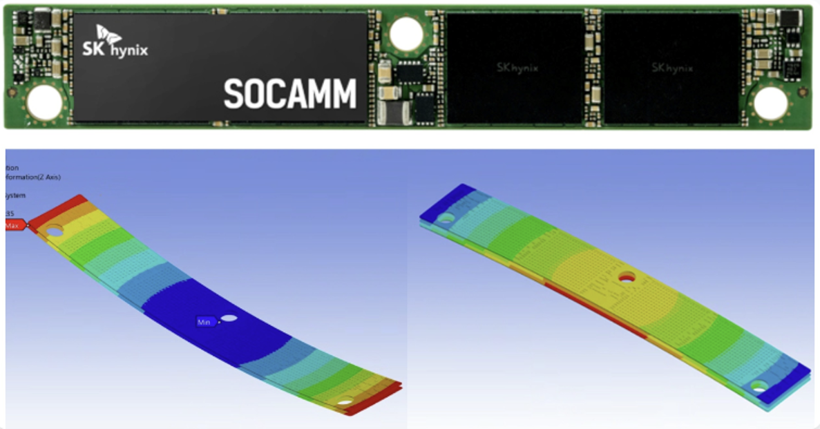
Warpage Measurement & Analysis
Experimental measurement of package-level warpage under thermal loading, followed by quantitative correlation with structural and material parameters.
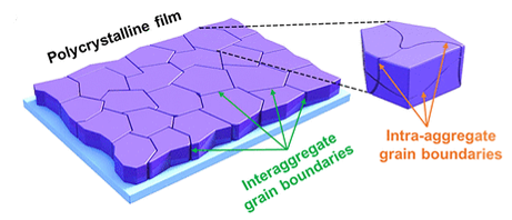
Thin-Film Microstructure Characterization
Investigation of microstructural evolution in thin films under different process conditions and its influence on mechanical properties.
Interfacial Property Measurement
Quantitative measurement of interfacial adhesion strength and viscoelastic properties for use as input parameters in reliability simulations.
Methodology
- Temperature-dependent warpage measurement systems
- Thin-film microstructure and mechanical property characterization
- Interfacial adhesion and viscoelastic property testing
Key Results & Impact
By incorporating experimentally measured material properties, the prediction error of package warpage was significantly reduced compared to conventional simulation approaches. This work improves the accuracy of reliability assessment and lifetime prediction for advanced semiconductor packaging.