Background & Motivation
As semiconductor packaging evolves toward higher integration and 3D architectures, thermal and structural interactions become increasingly complex. Temperature gradients, material mismatch, and process-induced stresses lead to warpage, interfacial delamination, and mechanical instability at both package and board levels. Accurate prediction of these behaviors requires multi-physics and multi-scale modeling frameworks that go beyond conventional simplified simulations.
Current Research Projects
Multi-Physics Thermo-Structural Modeling
Development of coupled thermal and structural simulation frameworks to capture nonlinear deformation and stress evolution in advanced semiconductor packages across multiple length scales.
Interfacial Delamination & Structural Stability Analysis
Numerical investigation of interfacial failure mechanisms, including delamination and local instability, driven by thermal loading and material mismatch in package and PCB-level structures.
Board-Level Reliability Simulation
Prediction of board-level reliability under thermal cycling, drop impact, and mechanical loading conditions using physics-based finite element modeling.
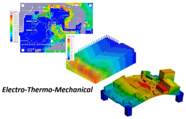
Methodology
- Coupled thermal–structural finite element modeling
- Multi-scale representation of package and board architectures
- Interfacial failure and stability criteria implementation
- Simulation of thermal cycling, drop, and mechanical loading conditions
Key Results & Impact
The proposed modeling framework enables accurate prediction of thermo-mechanical deformation, interfacial failure, and board-level reliability. These results support early-stage design optimization, reduce experimental iteration costs, and enhance the robustness of advanced semiconductor packaging systems.